I spy with my little eye developments towards a color-sensing ‘electric eye’

Refer a colleague
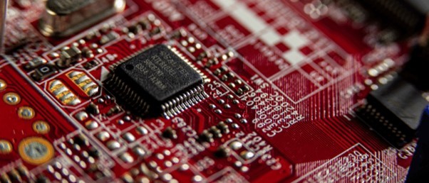
A team of researchers has made progress towards developing an ‘electric eye’ with improved color recognition, using a novel vertical stacking method to stack semiconducting materials.
Using nanotechnology to develop a device capable of mimicking aspects of neurobiology, researchers at Georgia State University (GA, USA) have provided nanorobotics with color vision. We’ve had color-sensing photoelectronics since the 70s; however, even with technological advances in the intervening decades, other hardware-limiting factors have prohibited further progress in the technology. For example, conventional sensors are built on space-intensive lateral layouts, which impairs color detection accuracy.
Enter van der Waals materials, an emergent experimental class of semiconductors – 2D materials that are stable and atomically thin. This includes graphene, the rockstar of the van der Waals material world, which offered new possibilities in 2D materials and nanotechnology, as well as its visually appealing hexagonal honeycomb structure.
This study utilized van der Waals semiconductors allowing the researchers to stack structures vertically, simultaneously simplifying the design of optical lens systems, but also providing more precise color recognition capabilities. This novel stacking architecture was achieved using ‘CuIn7Se11’ (CIS) and could mitigate the current limitations of downscaling color-sensing apparatus, opening new possibilities for artificial vision devices.
 Peering through the eyes of the proteus
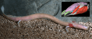
Researchers produce x-ray-computed microtomography scans of the endangered Proteus anguinus, a colorless serpentine that was believed to be a baby dragon in the 1600s.
Ningxin Li, the first author of the paper, elaborated: “Compared with conventional semiconductors, such as silicon, we can precisely control the van der Waals material band structure, thickness, and other critical parameters to sense the red, green, and blue colors.”
Semiconductors are fickle, their conductivity depends on a variety of factors including temperature, illumination, and magnetic fields. The conductivity of a semiconductor is also closely tied to its level of impurities – for reference, ten boron atoms per million silicon atoms is enough to increase its conductivity by a thousandfold.†
While the impurity-energy level relationships of conventional semiconductors such as silicon are effectively mapped, even the well-researched van der Waals semiconductors remain in comparatively uncharted territory. They may, however, constitute the most effective means of designing next-generation devices.
This research leads the way for biomimetic artificial vision devices, those that mimic biochemical processes using synthetic methods, and could one day result in technology for those with visual impairments.
Sidong Lei, who leads the research group, expounded on their efforts: “The ultimate purpose of our research is to develop a micro-scale camera for microrobots that can enter narrow spaces that are intangible by current means, and open up new horizons in medical diagnosis, environmental study, manufacturing, archaeology, and more.”
Please enter your username and password below, if you are not yet a member of BioTechniques remember you can register for free.


